Semiconductor and electronics manufacturing equipment operates at a level of precision that places material specifications outside the range that conventional structural materials can reliably meet. Nanometer-scale positioning tolerances, thermal stability across process temperature variations, cleanroom compatibility, and the dynamic performance demands of high-throughput wafer handling systems all impose requirements that drive material selection toward carbon fiber composite as the solution that most directly addresses the full combination of constraints. The challenge for semiconductor equipment OEMs evaluating carbon fiber is finding a composite manufacturer with the precision machining capability, process control, and engineering depth to deliver the dimensional accuracy and consistency these applications require. Contact our engineering team through our contact page or call 949-361-7580 to discuss your semiconductor equipment composite program.
Wafer handling robot arms and end effectors are among the most demanding structural applications for carbon fiber composites in semiconductor manufacturing. Every gram of mass at the end of a handling arm affects both the speed at which the arm can be accelerated and decelerated and the positional accuracy at the end of the motion cycle — the lighter the end effector, the faster the throughput and the more precise the placement, for a given motor and control system. Carbon fiber’s combination of low density and high stiffness-to-weight ratio makes it a strong candidate for wafer handling structural components where both dynamic performance and positional accuracy are primary design requirements.
The challenge for composite manufacturers supplying these components is producing the dimensional accuracy wafer-handling geometry requires across production runs, using post-cure machining that does not introduce residual stresses or dimensional variation the handling system’s tolerance budget cannot accommodate. CMI’s in-house 3/4/5 axis CAM machining capability supports post-cure dimensional accuracy at tight tolerances, as confirmed on our composite solutions page. Contact our engineering team through our contact page to discuss the dimensional requirements for your wafer-handling application.
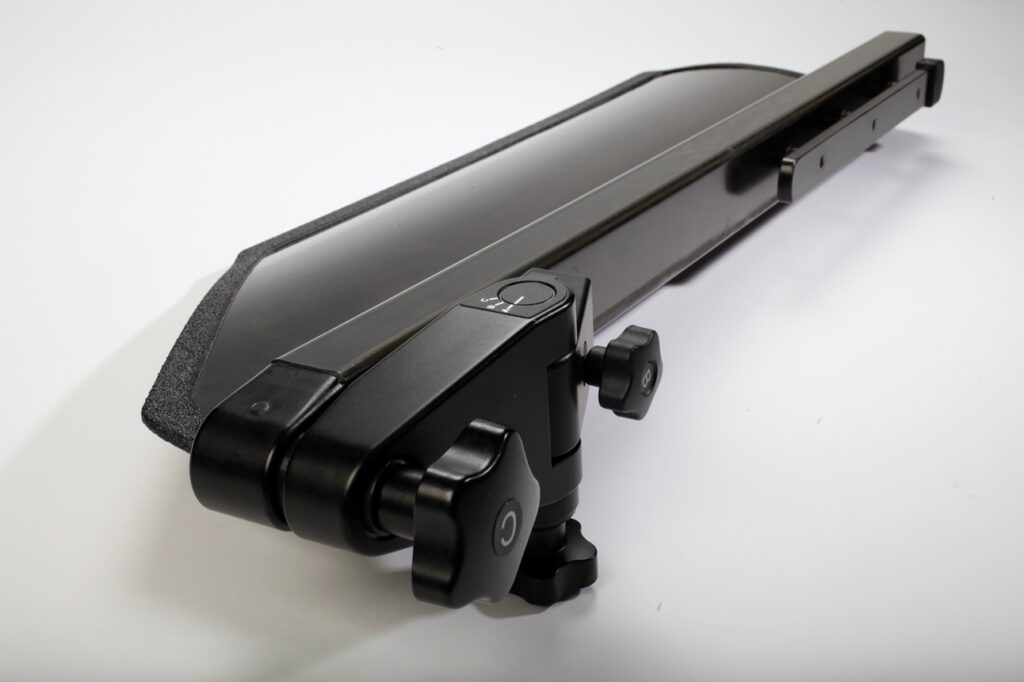
More detail on each of these capabilities is available on our composite solutions page, our in-house design and engineering page, and our composite manufacturing and assembly page. Contact our engineering team through our contact page to discuss your semiconductor equipment composite program.
The dimensional tolerances, thermal stability requirements, and cleanroom compatibility considerations of semiconductor equipment applications are best addressed early in the program. Factors such as laminate architecture, tooling design, machining strategy, and surface treatment specifications can be established during the design process and informed by both manufacturing experience and structural analysis.
CMI’s vertically integrated engineering and manufacturing capability supports semiconductor equipment programs from the earliest design stage through production delivery. Contact our engineering team through our contact page or call 949-361-7580 to discuss your application, or review our precision manufacturing capabilities on our composite solutions page.